
This document is a technical manual for Cypress Semiconductor Corporation's 4-Mb (256K x 18) Pipelined Sync SRAM CY7C1327F, introducing the product's features and characteristics, including registered inputs and outputs, 256K ×18 common I/O architecture, 3.3V / 2.5V I/O operation, fast clock-to-output times, high-performance 3-1-1-1 access rate, user-selectable burst counter, separate processor and controller address strobes, synchronous self-timed writes, asynchronous output enable, JEDEC-standard 100-pin TQFP and 119 Ball BGA packages, and “ZZ” Sleep Mode Option.
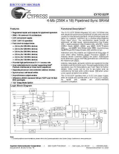
The CY7C1327F is a 4‑Mb (256K × 18) pipelined synchronous SRAM that operates from a +3.3 V core supply and supports both 3.3 V and 2.5 V I/O levels. It offers registered inputs and outputs for pipelined operation, fast clock‑to‑output times as low as 2.6 ns, and a selectable burst counter for Intel Pentium interleaved or linear burst sequences.
The device is offered in JEDEC‑standard 100‑pin TQFP and 119‑ball BGA packages. Detailed pin definitions, electrical characteristics, maximum ratings, and timing tables are provided to aid designers in integrating the SRAM into high‑performance systems.
| Memory size | 4 Mb (256K × 18) |
|---|---|
| Core supply voltage | 3.3 V |
| I/O supply voltage | 3.3 V or 2.5 V |
| Package options | 100‑pin TQFP, 119‑ball BGA |
The ZZ pin puts the SRAM into a power‑conservation sleep mode when asserted high.
Both 3.3 V and 2.5 V I/O supply voltages are supported.
The SRAM is available in 100‑pin TQFP and 119‑ball BGA packages.