
AS7C33128FT18B is a 3.3V 128K × 18 Flow Through Synchronous SRAM produced by Alliance Semiconductor. It has the following features: 131,072 words × 18 bits, Fast clock to data access: 6.5/7.5/8.0/10.0 ns, Fast OE access time: 3.5/4.0 ns, Fully synchronous flow through operation, Asynchronous output enable control, Economical 100-pin TQFP package, Individual byte write and Global write, Multiple chip enables for easy expansion, 3.3V core power supply, 2.5V or 3.3V I/O operation with separate VDDQ, Linear or interleaved burst control, Snooze mode for reduced power standby, Common data inputs and data outputs.
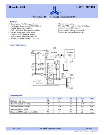
The AS7C33128FT18B is a high‑performance CMOS 2‑Mbit synchronous SRAM organized as 131,072 words × 18 bits. It offers fast clock‑to‑data access times (6.5‑10 ns), three chip‑enable inputs for easy expansion, and both linear and interleaved burst modes. The device supports 2.5 V or 3.3 V I/O operation with a separate Vppg supply and includes a snooze mode for low‑power standby.
The SRAM is supplied in an economical 100‑pin TQFP package and operates from a 3.3 V core supply (or 2.5 V for I/O). Absolute maximum ratings, recommended operating conditions, pin descriptions, and timing tables are provided for design reference. Ordering information and part‑number decoding are included at the end of the document.
| Organization | 131,072 words x 18 bits |
|---|---|
| Core power supply | 3.3 V |
| I/O supply voltage | 2.5 V or 3.3 V |
| Clock‑to‑data access time | 6.5/7.5/8.0/10.0 ns |
| Maximum operating current | 250 mA (3.3 V) |
| Maximum standby current | 120 mA (3.3 V) |
| Package | 100‑pin TQFP |
The core supply voltage is 3.3 V.
It is available in an economical 100‑pin TQFP package.
Maximum operating current is 250 mA and maximum standby current is 120 mA at 3.3 V.
The I/O pins can operate at either 2.5 V or 3.3 V.