
AS7C31026B 3.3 V 64K X 16 CMOS SRAM is a 6 T 0.18 u CMOS technology memory with industrial and commercial versions, center power and ground pins, high speed, low power consumption, TTL compatible, three-state I/O.
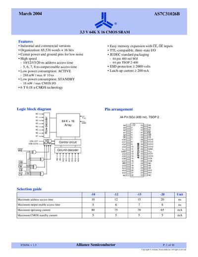
The AS7C31026B is a high‑performance 1 Mbit CMOS static RAM organized as 65,536 words × 16 bits. It offers fast address access times (10‑20 ns) and low power consumption (288 mW active, 18 mW standby) with TTL‑compatible I/O and multiple power/ground pins for low noise operation.
The document lists recommended operating conditions (3.0‑3.6 V supply, commercial temperature up to 70 °C, industrial up to 85 °C), absolute maximum ratings, timing parameters for read and write cycles, package dimensions for 44‑pin SOJ and TSOP 2, and ordering codes for commercial and industrial variants.
| Memory organization | 65,536 words × 16 bits (1 Mbit) |
|---|---|
| Supply voltage (VCC) | 3.0 V min, 3.3 V nominal, 3.6 V max |
| Address access time | 10 ns – 20 ns (depending on grade) |
| Output enable access time | 5 ns – 8 ns |
| Active power consumption | 288 mW max @ 10 ns |
| Standby power consumption | 18 mW max |
| ESD protection | 2000 V |
| Latch‑up current | 200 µA |
| Package options | 44‑pin SOJ (400 mil) and 44‑pin TSOP 2 |
The device operates from 3.0 V to 3.6 V, with a nominal 3.3 V supply.
It is offered in a 44‑pin SOJ (400 mil) and a 44‑pin TSOP 2 package.
Read address access times range from 10 ns to 20 ns, and output enable times from 5 ns to 8 ns.
Active power consumption is up to 288 mW at a 10 ns access time.