
This document describes the features and characteristics of the Cypress Semiconductor Corporation's 4-Mb (256K x 18) Pipelined Sync SRAM CY7C1327F, including registered inputs and outputs, 256K x 18 common I/O architecture, 3.3V core power supply, 3.3V/2.5V I/O operation, fast clock-to-output times, etc.
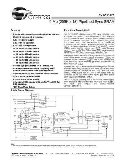
The CY7C1327F is a 4‑Mb (256K × 18) pipelined synchronous SRAM with registered inputs and outputs for high‑speed operation. It supports 3.3 V core power and 3.3 V/2.5 V I/O supplies, offers selectable burst modes, and is available in 100‑pin TQFP and 119‑ball BGA packages.
The document provides a complete functional description, pin definitions for both package types, timing diagrams for single‑read and single‑write cycles, sleep‑mode operation, and extensive electrical characteristics such as supply voltage ranges, output voltage levels, and maximum current ratings.
| Memory size | 4 Mb (256K × 18) |
|---|---|
| Core supply voltage | 3.3 V |
| I/O supply voltage | 3.3 V / 2.5 V |
| Maximum access time (250 MHz) | 2.6 ns |
| Package types | 100‑pin TQFP, 119‑ball BGA |
| Supply voltage (Vop) | 3.135 – 3.6 V |
The device operates from a +3.3 V core power supply.
The GW pin (Global Write Enable) is active LOW and writes all bytes when asserted.
It has three chip‑enable pins: CE1, CE2, and CE3.
The maximum access time is 2.6 ns for the 250‑MHz device.