
This document introduces the features of S71GS256/128N series MCP products in detail. The series products include one S29GL Flash memory die and one 1.8V pSRAM die. The power supply voltage range is 2.7V~3.1V, the VIO voltage range is 1.65V~1.95V, the package form is 8.0x11.6x1.2 mm FBGA (TLA084), and the working temperature range is -25°C~+85°C (Wireless).
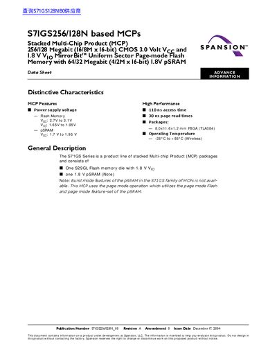
The S71GS256/128N is a stacked Multi‑Chip Product (MCP) that combines 256 Mb (or 128 Mb) MirrorBit™ Flash with 64 Mb (or 32 Mb) 1.8 V pSRAM in a compact FBGA package. It is intended for applications requiring high‑performance non‑volatile memory with integrated SRAM.
The document provides detailed electrical characteristics, timing diagrams, package dimensions, voltage ranges, and protection features. It also includes block diagrams, pin descriptions, and command sets for both Flash and pSRAM portions.
| Supply voltage (Flash) | 2 V – 3.1 V |
|---|---|
| Maximum access time (Flash) | 110 ns |
| Maximum page access time (Flash) | 30 ns |
| Operating temperature range | -25 °C to +85 °C |
| Package | 8.0 × 11.6 × 1.2 mm FBGA (TLA084) |
The device operates from –25 °C up to +85 °C.
It is housed in an 8.0 × 11.6 × 1.2 mm FBGA (TLA084) package.