
This document describes the features and characteristics of the S71GL032A MCP Flash Memory and RAM product. The flash memory has a capacity of 32 megabits and the RAM has capacities of 16/8/4 megabits. The flash memory operates at 3.0 volts and uses page mode. This product is under development, and readers are advised to contact the factory before designing with it.
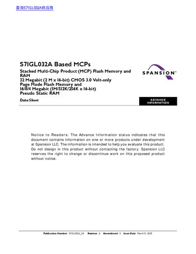
The S71GL032A is a stacked Multi‑Chip Product (MCP) that combines a 32‑Megabit Flash memory die with pseudo‑static RAM (pSRAM) or SRAM in a 56‑ball FBGA package. It operates from 2.7 V to 3.1 V and offers high‑performance access times of 100 ns for Flash and 70 ns for pSRAM/SRAM.
The document provides detailed specifications, pin descriptions, connection diagrams, and timing waveforms. It also includes ordering information, physical dimensions, and test conditions for designers evaluating the device.
| Flash Memory Density | 32 Mb |
|---|---|
| pSRAM Density | 4 Mb |
| Power Supply Voltage | 2.7 V to 3.1 V |
| Access Time (Flash) | 100 ns |
| Access Time (pSRAM/SRAM) | 70 ns |
| Package | 7 mm × 9 mm × 1.2 mm 56‑ball FBGA |
| Operating Temperature Range | -25 °C to +85 °C (standard) / -40 °C to +85 °C (extended) |
The device operates from 2.7 V to 3.1 V.
It is supplied in a 56‑ball fine‑pitch ball grid array (FBGA) measuring 7 mm × 9 mm × 1.2 mm.
The datasheet lists a 32‑Megabit flash memory density.
Flash access time is 100 ns, while pSRAM/SRAM access time is 70 ns.