
This document contains information on a product under development at Advanced Micro Devices. The information is intended to help you evaluate this product. AMD reserves the right to change or discontinue work on this proposed product without notice.
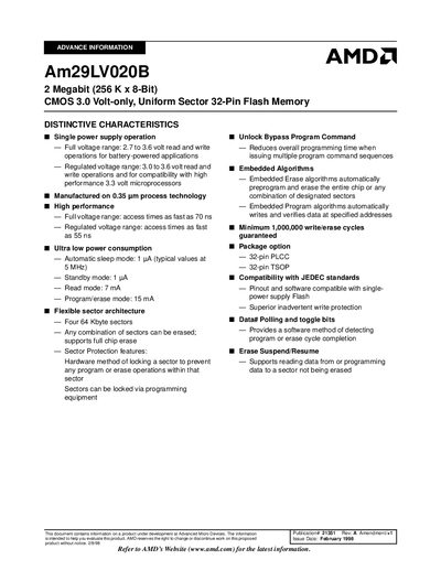
The Am29LV020B flash memory provides 2 Mbit (256 K × 8‑bit) storage in a single‑power‑supply design, supporting a full voltage range of 2.7 V to 3.6 V and a regulated range of 3.0 V to 3.6 V. It offers fast access times as low as 55 ns and low power consumption, with automatic sleep and standby modes.
The device is available in 32‑pin PLCC and 32‑pin TSOP packages, features flexible sector architecture with four 64 KB sectors, and includes hardware sector protection, erase‑suspend/resume, and data‑polling status bits for reliable programming and erasing.
| Memory size | 2 Megabit (256 K × 8‑bit) |
|---|---|
| Supply voltage (full range) | 2.7 V – 3.6 V |
| Supply voltage (regulated range) | 3.0 V – 3.6 V |
| Access time (fastest) | 55 ns |
| Read mode current | 7 mA |
| Program/erase mode current | 15 mA |
| Standby mode current | 1 pA |
| Automatic sleep mode current | 1 µA (typical) |
| Package options | 32‑pin PLCC, 32‑pin TSOP |
| Write/erase endurance | ≥ 1 000 000 cycles |
| Operating temperature range (commercial) | 0 °C – +70 °C |
| Operating temperature range (industrial) | -40 °C – +85 °C |
| Operating temperature range (extended) | -55 °C – +125 °C |
The Am29LV020B guarantees a minimum of one million write/erase cycles.
The device is offered in 32‑pin PLCC and 32‑pin TSOP packages.
By reading the DQ7 (Data# Polling) and DQ6 (toggle) status bits.