
Am28F010 1 Megabit (128 K x 8-Bit) CMOS 12.0 Volt, Bulk Erase Flash Memory is a high-performance, low-power Flash memory that is compatible with JEDEC-standard byte-wide 32-Pin EPROM pinouts. It has a minimum of 10,000 write/erase cycles and can be erased and programmed at 12.0 V ±5% voltage.
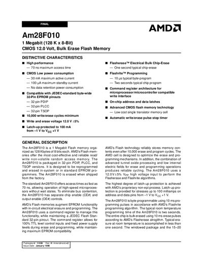
The Am28F010 is a 1 Megabit (128 K × 8‑bit) CMOS flash memory offered in 32‑pin PDIP, PLCC and TSOP packages. It provides high‑performance operation with a maximum access time of 70 ns, low power consumption (30 mA active, 100 pA standby) and latch‑up protection up to 100 mA.
The device supports in‑system electrical erase and programming using a 12.0 V + 5 % high‑voltage input. Typical chip‑erase time is under one second, while a byte can be programmed in about 10 µs and the whole chip in roughly two seconds. It is rated for at least 10 000 write/erase cycles and operates over commercial, industrial or extended temperature ranges.
| Memory Capacity | 1 Megabit (128 K × 8 bits) |
|---|---|
| Maximum Access Time | 70 ns |
| Active Current | 30 mA (max) |
| Standby Current | 100 pA (max) |
| Write/Erase Cycles | ≥ 10 000 cycles |
| Write Voltage | 12.0 V + 5 % |
| Latch‑up Protection | 100 mA from –1 V to VCC + 1 V |
| Typical Chip‑Erase Time | < 1 s |
| Typical Byte‑Program Time | 10 µs |
| Typical Chip‑Program Time | ≈ 2 s |
| Operating Temperature (Commercial) | 0 °C to +70 °C |
| Operating Temperature (Industrial) | -40 °C to +85 °C |
| Operating Temperature (Extended) | -55 °C to +125 °C |
| Package Types | 32‑pin PDIP, PLCC, TSOP |
| Speed Options | 70 ns, 90 ns, 120 ns, 150 ns, 200 ns |
The maximum access time is 70 ns.
It is rated for at least 10 000 write/erase cycles.
A typical chip‑erase completes in less than one second.
Programming uses a 12.0 V + 5 % high‑voltage input (Vpp).