
This document provides information on a product under development at Advanced Micro Devices. The product is a stacked multi-chip package (MCP) flash memory and SRAM. It features high performance and a flexible architecture.
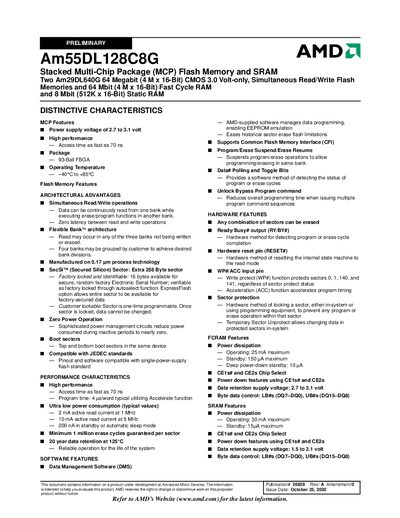
The Am55DL128C8G is a stacked multi‑chip package (MCP) that combines two 64‑Mbit flash memory devices and an 8‑Mbit static RAM. It operates from a single 2.7 V to 3.1 V supply and supports simultaneous read/write operations with zero latency, making it suitable for high‑performance embedded applications.
Key features include an access time as fast as 70 ns, ultra‑low power consumption (2 mA active read at 1 MHz, 200 nA standby), a 93‑ball FBGA package, and a temperature range of –40 °C to +85 °C. The device also offers a Secured Silicon (SecSi) sector for secure data storage and supports JEDEC‑standard command sets.
| Power supply voltage | 2.7 V to 3.1 V |
|---|---|
| Access time | 70 ns (typical) |
| Active read current (1 MHz) | 2 mA |
| Standby current | 200 nA |
| Erase cycles per sector | ≥ 1 million |
| Data retention | 20 years at 125 °C |
| Package type | 93‑Ball FBGA |
| Operating temperature range | -40 °C to +85 °C |
| Flash memory size | 64 Mbit (4 M × 16‑bit) |
| SRAM size | 8 Mbit (512 K × 16‑bit) |
The device provides an access time as fast as 70 ns.
It operates from 2.7 V to 3.1 V.
A minimum of 1 million erase cycles is guaranteed per sector.
The standby current is 200 nA in standby or automatic sleep mode.