
This document contains information about the features and characteristics of a product under development at Advanced Micro Devices, including single power supply operation, high performance, ultra low power consumption, and flexible sector architecture.
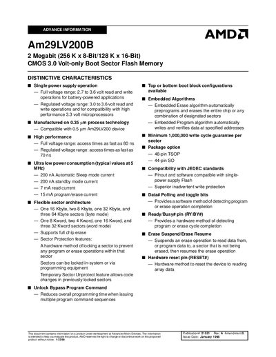
The Am29LV200B is a 2 Megabit CMOS flash memory offered in 44‑pin SO and 48‑pin TSOP packages. It operates with a single 3.0 V power supply and supports both full (2.7‑3.6 V) and regulated (3.0‑3.6 V) voltage ranges for read and write operations. The device features fast access times (70 ns regulated, 80 ns full), ultra‑low power consumption, and flexible sector architecture with built‑in erase and program algorithms.
The handbook includes detailed pin configurations, connection diagrams, ordering information, and temperature range options (commercial, industrial, extended). It also describes hardware reset, ready/busy signaling, and sector protection features, making it suitable for high‑performance microprocessor applications.
| Memory density | 2 Megabit (256 K × 8‑Bit/128 K × 16‑Bit) |
|---|---|
| Supply voltage | 3.0 V‑only |
| Full voltage range | 2.7 V to 3.6 V |
| Regulated voltage range | 3.0 V to 3.6 V |
| Access time (regulated) | 70 ns |
| Access time (full) | 80 ns |
| Automatic Sleep mode current | 200 nA |
| Standby mode current | 200 nA |
| Read current | 7 mA |
| Program/Erase current | 15 mA |
| Package options | 48‑pin TSOP, 44‑pin SO |
| Temperature range (commercial) | 0 °C to +70 °C |
| Temperature range (industrial) | -40 °C to +85 °C |
| Temperature range (extended) | -55 °C to +125 °C |
| Write‑cycle endurance | ≥ 1,000,000 cycles per sector |
The device guarantees at least 1,000,000 write cycles per sector.
The RY/BY# pin provides a hardware method of detecting program/erase cycle completion.
It is offered in a 48‑pin TSOP package and a 44‑pin SO package.