
Am28F512A is a 512 Kbit Flash memory with high performance, low power consumption, and compatibility with JEDEC standards.
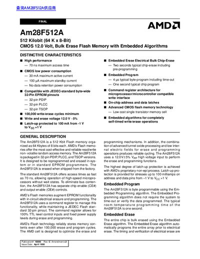
The Am28F512A is a 512‑Kbit (64 K × 8‑bit) CMOS flash memory device offering high‑performance operation with a maximum access time of 70 ns and low power consumption. It supports 100,000 write/erase cycles, latch‑up protection, and can be programmed or erased in‑system using a 12 V high‑voltage input.
The document includes pin‑out diagrams for 32‑pin PDIP, PLCC, and TSOP packages, ordering information, detailed pin descriptions, and explanations of the embedded erase and programming algorithms. Physical dimensions, temperature ranges, and revision history are also provided.
| Memory size | 512 Kilobit (64 K x 8‑Bit) |
|---|---|
| Maximum access time | 70 ns |
| Supply voltage | 12.0 V CMOS |
| Active current | 30 mA maximum |
| Standby current | 100 µA maximum |
| Write/erase cycles | ≥ 100,000 cycles |
| Erase/program voltage | 12.0 V ± 5 % |
| Latch‑up protection | 100 mA from –1 V to VEE + 1 V |
| Package types | 32‑pin PDIP, PLCC, TSOP |
| Temperature range (Industrial) | -40 °C to +85 °C |
The device has a maximum access time of 70 ns.
It is rated for at least 100,000 write/erase cycles.
A 12.0 V high‑voltage input with a ±5 % tolerance is required.
The device is offered in 32‑pin PDIP, PLCC, and TSOP packages.