
This document describes a 12 LVPECL/24 CMOS output clock generator with an integrated 2.5 GHz VCO. It supports external 3.3V/5V VCO/VCXO up to 2.4 GHz. The clock generator features a low phase noise phase-locked loop (PLL), accepts CMOS, LVDS, or LVPECL reference signals up to 250 MHz, supports automatic and manual reference switchover/holdover modes, and has 12 1.6 GHz LVPECL outputs with low additive output jitter.
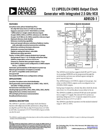
The AD9520-1 provides a multi‑output clock distribution function with sub‑picosecond jitter performance. It integrates a PLL and an on‑chip VCO that tunes from 2.27 GHz to 2.65 GHz, and can also use an external VCO/VCXO up to 2.4 GHz. The device offers twelve LVPECL outputs (configurable as CMOS) organized in four groups, each with programmable dividers and phase delay.
Typical applications include low‑jitter clock distribution for high‑speed serial links (SONET, 10 GbE, etc.), clocking of high‑performance ADCs/DACs, wireless transceivers, and test equipment. The AD9520-1 operates from a single 3.3 V supply over an industrial temperature range (‑40 °C to +85 °C).
| VCO Frequency Range | 2.27–2.65 GHz |
|---|---|
| Phase Noise @ 1 kHz Offset | -50 dBc/Hz |
| Maximum LVPECL Output Frequency | 2.4 GHz |
| Power Supply Voltage (VS) | 3.135 V – 3.465 V (typical 3.3 V) |
| Reference Input Frequency Range | 0 – 250 MHz |
| Additive Output Jitter | as low as 225 fs rms |
| Channel‑to‑Channel Skew (grouped outputs) | < 16 ps |
The on‑chip VCO tunes from 2.27 GHz to 2.65 GHz.
It provides twelve LVPECL outputs organized in four groups.
The LVPECL outputs can operate up to 2.4 GHz.
The device runs from a 3.3 V supply, with VS allowed from 3.135 V to 3.465 V.