
ZXFV4089 is a low-distortion video amplifier and DC restoration circuit. It is specially designed to provide brightness level stability as a 'black-level clamp' in video systems with very low distortion and low power consumption. A high fidelity video amplifier is combined with a sample-hold switch circuit using an external coupling capacitor to provide level-shifting of the video output such that a time-gated sample of the waveform is set to be equal to an external reference voltage (usually zero voltage). A buffered TTL/CMOS logic input signal controls the switch. The gain is set externally by two resistors. In a typical application, the sample-hold circuit is gated on during part of the back-porch interval of an analog video waveform. Then the video waveform is stabilised for the remainder of the line-scan interval.
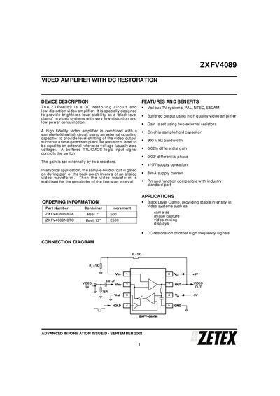
The ZXFV4089 is a low‑distortion video amplifier with an integrated sample‑hold circuit that provides DC restoration and black‑level clamping for PAL, NTSC and SECAM TV systems. Gain is set by two external resistors and the device operates from a ±5 V supply with low power consumption.
The document provides absolute maximum ratings, detailed electrical characteristics, operating notes, and package dimensions for the SO‑16 package, along with ordering information and recommended layout guidelines for high‑speed analog circuits.
| Bandwidth | 300 MHz |
|---|---|
| Differential Gain | 0.02 % |
| Differential Phase | 0.02° |
| Supply Voltage | 4 V / -5 V |
| Supply Current | 8 mA |
| Output Current (pin 7) | 60 mA |
| Input Offset Voltage | 10 mV |
| Open Loop Gain | 48‑61 dB |
The device has a -3 dB bandwidth of 300 MHz.
It operates from a dual supply of +4 V and –5 V.
Gain is set externally by two resistors.
The maximum output current on pin 7 is 60 mA.