
The ZXGD3002E6 is a high-speed non-inverting single MOSFET gate driver capable of driving up to 9A into a MOSFET or IGBT gate capacitive load from supply voltages up to 20V. With typical propagation delay times down to 2ns and rise/fall times down to 11ns this device ensures rapid switching of the power MOSFET or IGBT to minimize power losses and distortion in high current fast switching applications. The ZXGD3002E6 is inherently rugged to latch-up and shoot-through, and its wide supply voltage range allows full enhancement to minimize on-losses of the power MOSFET or IGBT. Its low input voltage requirement and high current gain allows high current driving from low voltage controller ICs, and the optimized pin-out SOT23-6 package with separate source and sink pins eases board layout, enabling reduced parasitic inductance and independent control of rise and fall slew rates.
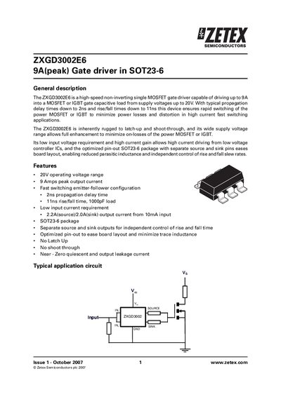
The ZXGD3002E6 is a high‑speed non‑inverting single MOSFET gate driver capable of delivering up to 9 A peak output current from supply voltages up to 20 V. It features a fast propagation delay of about 2 ns, rise/fall times of 11 ns into a 1000 pF load, low input current, and separate source and sink pins to simplify board layout.
Typical applications include synchronous switch‑mode power supplies, secondary‑side synchronous rectification, plasma‑display‑panel power modules, motor‑control circuits, and audio‑amplifier output stages. The device is supplied in a compact SOT‑23‑6 package with a maximum power dissipation of 11 W and a junction‑to‑ambient thermal resistance of 113 °C/W.
| Operating voltage range | 0‑20 V |
|---|---|
| Peak output current | 9 A |
| Propagation delay | 2 ns |
| Rise/fall time (1000 pF load) | 11 ns |
| Source output current (10 mA input) | 2.2 A |
| Sink output current (10 mA input) | 2.0 A |
The device can deliver a peak output current of 9 A.
The propagation delay is about 2 ns.
It is supplied in a SOT‑23‑6 surface‑mount package.
The device can operate up to 20 V supply voltage.