
This data sheet provides detailed information on the features and characteristics of the SST31LF041/041A/043/043A Monolithic Flash + SRAM ComboMemory
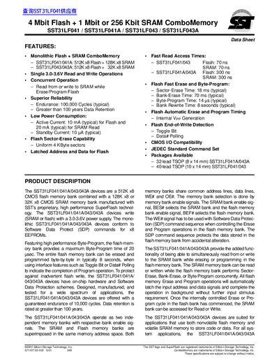
The SST31LF041/041A/043/043A devices combine a 512 Kbit x8 Flash memory with either a 128 Kbit x8 SRAM (041/041A) or a 32 Kbit x8 SRAM (043/043A) in a single monolithic package. They operate from a single 3.0‑3.6 V supply and support concurrent SRAM read/write while Flash is being programmed or erased, providing high reliability and low power consumption.
Key specifications include typical active currents of 10 mA for Flash and 20 mA for SRAM reads, standby current of 10 µA, endurance of 100 000 cycles, data retention over 100 years, 70 ns read access times, 18 ms sector‑erase time, 14 µs byte‑program time, and uniform 4 KB sectors. The devices are offered in 32‑lead and 40‑lead TSOP packages and use standard JEDEC command sets for Flash operations.
| Flash size | 512 Kbit x8 |
|---|---|
| SRAM size (041/041A) | 128 Kbit x8 |
| SRAM size (043/043A) | 32 Kbit x8 |
| Operating voltage | 3.0‑3.6 V |
| Active current (Flash) | 10 mA (typical) |
| Active current (SRAM read) | 20 mA (typical) |
| Standby current | 10 µA (typical) |
| Endurance | 100 000 cycles (typical) |
| Data retention | >100 years |
| Flash read access time | 70 ns |
| Sector‑erase time | 18 ms (typical) |
| Byte‑program time | 14 µs (typical) |
| Sector size | 4 KB |
The device operates from a single 3.0 V to 3.6 V supply.
Typical active current for Flash reads is 10 mA.
A sector erase typically completes in 18 ms.
Yes, the device allows concurrent SRAM read/write during Flash erase or program operations.