
This document describes the parameters such as VDS, Tjmax, and the features and characteristics of the product.
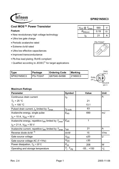
The SPW21N50C3 is a 560 V Cool MOS power transistor featuring ultra‑low gate charge, low on‑state capacitances and high avalanche capability. It is RoHS compliant and qualified for target applications according to JEDEC standards.
Key specifications include a continuous drain current of 21 A at 25 °C, pulsed current up to 63 A, power dissipation of 208 W, thermal resistance junction‑to‑case of 0.6 K/W, and typical on‑state resistance of 0.16 Ω. Electrical parameters such as gate threshold voltage (2.1‑3.9 V), input capacitance (2400 pF) and output capacitance (1200 pF) are also listed.
| Maximum Drain‑Source Voltage | 560 V |
|---|---|
| Pulsed Drain Current | 63 A |
| Power Dissipation (Pd) at 25 °C | 208 W |
| Avalanche Energy (single pulse) | 690 mJ |
It can dissipate up to 208 W when the case temperature is 25 °C.