
The IPB50CN10N G IPD49CN10N G IPI50CN10N G IPP50CN10N G OptiMOS®2 Power-Transistor features the following: N-channel, normal level; Excellent gate charge x R DS(on) product (FOM); Very low on-resistance R DS(on); 175 °C operating temperature; Pb-free lead plating; RoHS compliant; Qualified according to JEDEC1) for target application; Ideal for high-frequency switching and synchronous rectification.
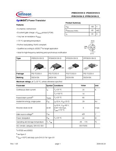
The OptiMOS®2 power‑transistor family from Infineon includes the IPB50CN10N G, IPD49CN10N G, IPI50CN10N G and IPP50CN10N G devices. These N‑channel MOSFETs are designed for high‑frequency switching and synchronous rectification, offering low on‑resistance, high current capability and operation up to 175 °C.
The handbook provides comprehensive electrical characteristics (drain current, breakdown voltage, gate charge), thermal data, dynamic switching parameters and mechanical dimensions for the four package types (PG‑TO220‑3, PG‑TO252‑3, PG‑TO263‑3, PG‑TO262‑3). It also includes safety and legal notices required for component use.
| Continuous drain current (Id) at 25 °C | 20 A |
|---|---|
| Pulsed drain current (Id, pulsed) | 80 A |
| Drain‑source breakdown voltage (Vds) | 100 V |
| Gate threshold voltage (Vgs(th)) | typical 2 V |
| On‑state resistance (Rds(on)) | typical 49 mΩ |
| Operating temperature range | -55 °C to 175 °C |
| Package types | PG‑TO220‑3, PG‑TO252‑3, PG‑TO263‑3, PG‑TO262‑3 |
The maximum continuous drain current is 20 A at a junction temperature of 25 °C.
They are rated for operation from –55 °C up to 175 °C.
Package outlines are given for PG‑TO220‑3, PG‑TO252‑3, PG‑TO263‑3 and PG‑TO262‑3.
The total gate charge is typically between 12 nC and 16 nC.