
This document describes the features and characteristics of the MAX5062/MAX5063/MAX5064 high-frequency, 125V half-bridge, n-channel MOSFET drivers, suitable for high-power, high-frequency telecom power converters.
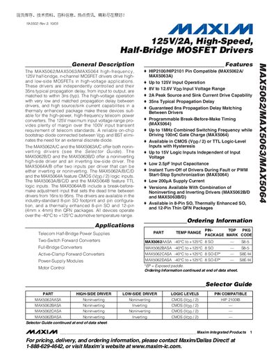
The MAX5062, MAX5063 and MAX5064 are 125 V, 2 A high‑speed half‑bridge MOSFET drivers designed for telecom power converters and motor‑control applications. They feature independently controlled high‑ and low‑side drivers with typical 35 ns propagation delay and matched timing within 3 ns.
These devices are offered in 8‑Pin SO, thermally enhanced 8‑Pin SO, and 12‑Pin thin QFN packages and operate over an automotive temperature range of –40 °C to +125 °C. Applications include two‑switch forward converters, full‑bridge converters, active‑clamp forward converters, power‑supply modules, and motor‑control circuits.
| Maximum Input Voltage | 125 V |
|---|---|
| Peak Source/Sink Current | 2 A |
| Typical Propagation Delay | 35 ns |
| Operating Temperature Range | –40 °C to +125 °C |
The typical propagation delay is 35 ns.
The drivers are rated for a maximum input voltage of 125 V.
Each driver can source and sink up to 2 A peak current.