
The MAX2055 evaluation kit is a tool for evaluating the MAX2055 high-linearity, digitally controlled, variable-gain analog-to-digital converter (ADC) driver/amplifier (DVGA). The kit is fully assembled and tested at the factory, enabling users to quickly evaluate it in the laboratory. It features a frequency range of 30MHz to 300MHz, variable gain from -3dB to +20dB, output IP3 of 40dBm (all gain settings at 70MHz), -76dBc second harmonic, -69dBc third harmonic, and other characteristics.
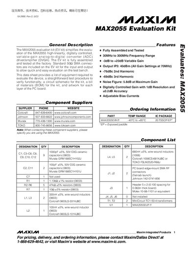
The MAX2055 evaluation kit is a fully assembled, factory‑tested board that simplifies evaluation of the MAX2055 high‑linearity, digitally controlled variable‑gain ADC driver. It includes SMA connectors, a 20‑pin TSSOP‑EP package, and a range of components such as inductors, capacitors, and transformers to support operation from 30 MHz to 300 MHz with gain from –3 dB to +20 dB.
The manual offers a quick‑start guide, detailed test procedures, and layout considerations. It explains how to connect power and RF ports, set gain via header pins, measure supply current and power gain, and modify the kit for single‑ended operation. Schematic diagrams and PCB layout figures help users design their own boards based on the evaluation kit.
| Frequency Range | 30 MHz to 300 MHz |
|---|---|
| Variable Gain | -3 dB to +20 dB |
| Output IP3 | 40 dBm (at 70 MHz) |
| Noise Figure | 5.8 dB at maximum gain |
| Operating Temperature Range | -40 °C to +85 °C |
| IC Package | 20‑lead TSSOP‑EP |
When powered at +5 V, the kit draws approximately 250 mA.
The MAX2055 operates from 30 MHz up to 300 MHz.
Connect the header pins B4‑B0 to GND to select maximum gain (about 20 dB).
Inductor L2 should have a DC resistance less than 0.2 Ω.