
The MAX2051 high-linearity, up/downconversion mixer provides +35dBm input IP3, 7.8dB noise figure (NF), and 7.4dB conversion loss for 850MHz to 1550MHz wireless infrastructure and multicarrier cable head-end downstream video, video-on-demand (VOD), and cable modem termination systems (CMTS) applications. The MAX2051 also provides excellent suppression of spurious intermodulation products (> 77dBc at an RF level of -14dBm), making it an ideal downconverter for DOCSIS® 3.0 and Euro DOCSIS cable head-end systems. With an LO circuit tuned to support frequencies ranging from 1200MHz to 2250MHz, the MAX2051 is ideal for high-side LO injection applications over an IF frequency range of 50MHz to 1000MHz. In addition to offering excellent linearity and noise performance, the MAX2051 also yields a high level of component integration. The device integrates baluns in the RF and LO ports, which allow for a single-ended RF input and a single-ended LO input. The MAX2051 requires a typical LO drive of 0dBm and a supply current guaranteed to below 130mA. The MAX2051 is available in a compact 5mm x 5mm, 20-pin thin QFN package with an exposed pad. Electrical performance is guaranteed over the extended temperature range, from TC = -40°C to +85°C.
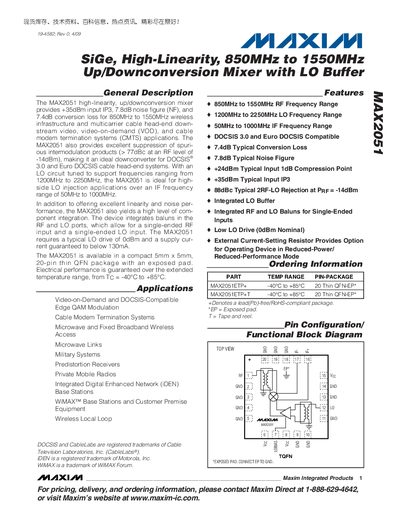
The MAX2051 mixer provides high linearity and low noise for 850 MHz‑1550 MHz RF applications, supporting LO frequencies from 1.2 GHz to 2.25 GHz and IF outputs from 50 MHz to 1 GHz. It integrates RF and LO baluns, requires a typical LO drive of 0 dBm, and is supplied at 5 V with a maximum current of 130 mA.
The device is offered in a 20‑pin thin QFN‑EP package (5 mm × 5 mm) with an exposed pad that must be connected to the PCB ground plane for thermal and RF performance. Electrical specifications are guaranteed over –40 °C to +85 °C, and the datasheet includes detailed absolute‑maximum ratings, DC/AC characteristics, and layout recommendations.
| RF Frequency Range | 850 MHz – 1550 MHz |
|---|---|
| LO Frequency Range | 1200 MHz – 2250 MHz |
| IF Frequency Range | 50 MHz – 1000 MHz |
| Typical Conversion Loss | 7.4 dB |
| Typical Noise Figure | 7.8 dB |
| Typical Input IP3 | +35 dBm |
| Typical Input 1 dB Compression Point | +24 dBm |
| 2RF‑LO Spurious Rejection (at PRF = –14 dBm) | 88 dB |
| Supply Voltage (VCC) | 4.75 V – 5.25 V |
| Supply Current | 105 mA – 130 mA |
| Package | 20‑pin thin QFN‑EP, 5 mm × 5 mm |
| Operating Temperature Range | -40 °C to +85 °C |
The device requires a typical LO drive of 0 dBm.
The exposed pad must be connected to the ground plane of the PCB, preferably with multiple vias.
The typical supply current is up to 130 mA.
RF and LO inputs must stay within –0.3 V to +5.5 V relative to ground.