
K5L5628JT(B)M is a 256M Bit (16M x16) Synchronous Burst , Multi Bank NOR Flash / 128M Bit(8M x16) Synchronous Burst UtRAM launched by Samsung
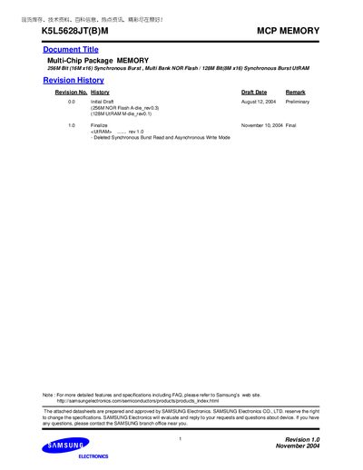
The K5L5628JT(B)M is a Multi‑Chip Package (MCP) memory that combines a 256Mbit synchronous burst multi‑bank NOR Flash with a 128Mbit synchronous burst UtRAM. It is targeted for mobile communication systems where reduced board area and low power consumption are critical.
Key specifications include a -30 °C to 85 °C operating temperature range, 115‑ball FBGA package (8.0 mm × 12.0 mm), dual‑voltage operation (1.7‑1.95 V for NOR, 2.5‑2.7 V for UtRAM), burst access times as low as 14.5 ns, and power consumption of 30 mA (burst) and 15 mA (program/erase). The device supports various burst modes, block protection, and power‑saving features such as Partial Array Refresh.
| Operating Temperature | -30°C ~ 85°C |
|---|---|
| Package Type | 115‑ball FBGA, 8.0 mm × 12.0 mm |
| NOR Flash Voltage | 1.7 V to 1.95 V (Read/Write) |
| UtRAM Voltage | 2.5 V to 2.7 V (Vcc), 1.7 V to 2.0 V (Veca) |
| Burst Access Time (54 MHz) | 14.5 ns |
| Initial Access Time (54 MHz) | 88.5 ns |
| Program/Erase Current | 15 mA |
| Burst Access Current | 30 mA |
| Standby / Auto‑Sleep Current | 25 µA |
| Endurance | 100 k program/erase cycles |
| Data Retention | 10 years |
| Maximum Burst Clock Frequency | 52.9 MHz |
It operates from –30 °C to 85 °C.
The device uses a 115‑ball FBGA package measuring 8.0 mm × 12.0 mm.
Burst access current is 30 mA, while program/erase current is 15 mA.
It is rated for at least 100 k program/erase cycles.