
This document introduces the features and characteristics of 1Gb DDR SDRAM, including voltage, data transmission speed, interface type, etc.
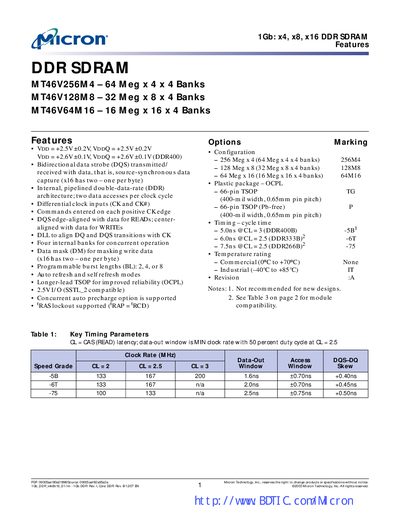
The document describes Micron's 1 Gb DDR SDRAM family offered in three configurations: 64 Mbit (MT46V256M4) with a 4‑bank x4 organization, 32 Mbit (MT46V128M8) with a 4‑bank x8 organization, and 16 Mbit (MT46V64M16) with a 4‑bank x16 organization. All parts use a double‑data‑rate architecture, differential clock inputs, and support programmable burst lengths of 2, 4, or 8.
Key sections cover functional description, timing parameters, address mapping, speed‑grade compatibility, pin assignments for the 66‑pin TSOP package, state diagrams, and power‑down operation. The datasheet also lists temperature ratings (commercial 0 °C‑70 °C, industrial 40 °C‑85 °C) and electrical specifications such as supply voltages and CAS latency values.
| Capacity (MT46V256M4) | 64 Mbit (4 banks × 4) |
|---|---|
| Capacity (MT46V128M8) | 32 Mbit (4 banks × 8) |
| Capacity (MT46V64M16) | 16 Mbit (4 banks × 16) |
| Supply Voltages | VDD ≈ 4.2 V, VDDQ ≈ 4.0 V |
| CAS latency (DDR400) | CL = 3 (5.0 ns) |
| Package | 66‑pin TSOP |
| Data Bus Width | x4, x8, x16 |
The DDR SDRAM supports programmable burst lengths of 2, 4, or 8 locations.
The parts are supplied in a 66‑pin TSOP package.