
The ADG3123 is an 8-channel, noninverting CMOS to high voltage level translator. It operates in the input voltage range of 2.3V to 5.5V and provides output voltage levels from -24.4V to +35V. The device features low power consumption, fast rise/fall time, propagation delay, and is suitable for low voltage to high voltage translation applications such as TFT-LCD panels and piezoelectric motor drivers.
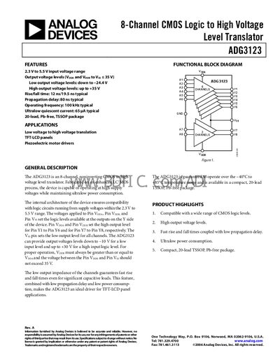
The ADG3123 is an 8‑channel, non‑inverting CMOS‑to‑high‑voltage level translator designed for low‑voltage to high‑voltage translation in applications such as TFT‑LCD panels and piezoelectric motor drivers. It operates from 2.3 V to 5.5 V input levels and can output voltages up to +35 V and down to –24.4 V while consuming ultralow quiescent current.
The document includes detailed specifications, absolute maximum ratings, pin configuration, typical performance curves, and ordering information. It also provides application guidance, a functional block diagram, and ESD handling recommendations for designers integrating the device into their circuits.
| Input voltage range | 2.3 V to 5.5 V |
|---|---|
| Output high voltage (Y1‑Y6) | up to +35 V |
| Output low voltage (Y1‑Y8) | down to –24.4 V |
| Rise time (typical) | 12 ns |
| Fall time (typical) | 19.5 ns |
| Propagation delay (typical) | 80 ns |
| Operating frequency (typical) | 100 kHz |
| Quiescent current | 65 pA |
| Package | 20‑lead TSSOP, Pb‑free |
The device accepts input voltages from 2.3 V to 5.5 V.
The typical quiescent current is 65 pA.
It is supplied in a 20‑lead thin‑shrink small outline package (TSSOP), Pb‑free.
The typical maximum operating frequency is 100 kHz.