
This product is a 2.5V/3.3V, 2:1 multiplexer/demultiplexer bus switch
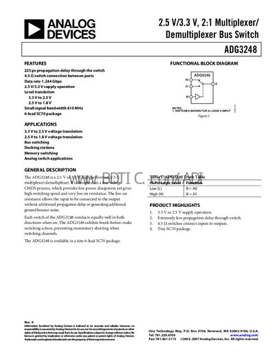
The ADG3248 is a 2.5 V‑3.3 V, 2:1 multiplexer/demultiplexer bus switch built on a low‑voltage CMOS process. It offers very low on‑resistance, fast switching (225 ps propagation delay) and supports level translation between 3.3 V, 2.5 V and 1.8 V domains. The device features break‑before‑make operation to prevent shorting when switching channels and is supplied in a tiny 6‑lead SC70 package.
Typical applications include voltage translation, bus switching for docking stations, memory bank switching and general analog switch functions. The datasheet provides detailed specifications, pin descriptions, performance curves, and ordering information for designers.
| Propagation delay | 225 ps |
|---|---|
| Supply voltage range (VCC) | 2.3 V to 3.6 V |
| Package | 6‑lead SC70 (SC70) package |
The device has a propagation delay of 225 ps through the switch.
It operates from 2.3 V up to 3.6 V supply voltage.
It is offered in a 6‑lead SC70 (thin‑shrink small outline transistor) package.