
The ADF4002 frequency synthesizer is used to implement local oscillators in the upconversion and downconversion sections of wireless receivers and transmitters. It features a 400 MHz bandwidth, 2.7V to 3.3V power supply, extended tuning voltage in 3V systems, programmable charge pump currents, 3-wire serial interface, analog and digital lock detect, and more.
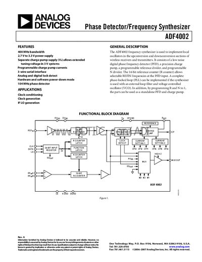
The ADF4002 is a high‑performance frequency synthesizer IC designed for clock conditioning, generation, and IF/LO applications in wireless receivers and transmitters. It integrates a low‑noise digital phase‑frequency detector, programmable charge pump, reference divider, and N‑divider, allowing PLL implementation with an external loop filter and VCO.
This handbook provides a complete description of the device, including functional block diagrams, pin configurations, electrical specifications, timing characteristics, thermal data, and ordering information, enabling designers to integrate the part into their systems.
| Analog power supply voltage (AVop) | 2.7 V to 3.3 V |
|---|---|
| Phase detector frequency | 104 MHz |
| RF input frequency range | 5 MHz to 400 MHz |
| Reference input frequency range | 20 MHz to 300 MHz |
| Operating temperature range (Industrial B version) | -40 °C to +85 °C |
The device operates from –40 °C to +85 °C (Industrial B version).
The maximum charge‑pump output current is 5 mA when Rser = 5.1 kΩ.
Pin 2 (CP) is the charge‑pump output pin.