
The AD9517-0 is a 12-output clock generator with an integrated 2.8 GHz VCO. It features low phase noise and a phase-locked loop. The chip's VCO frequency range is 2.55 GHz to 2.95 GHz, and it supports external VCO/VCXOs up to 2.4 GHz. It can accept 1 differential or 2 single-ended reference inputs, and it supports reference monitoring capabilities. It has automatic and manual reference switchover/holdover modes and can automatically recover from holdover. It supports references up to 250 MHz, and it can provide programmable delays in the path to the PFD. It supports digital or analog lock detect, which can be selected.
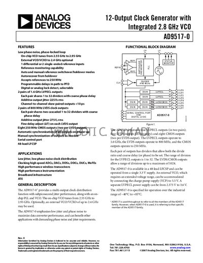
The AD9517-0 is a 12‑output clock generator that integrates a 2.8 GHz VCO and a PLL. It offers low phase‑noise and low jitter performance for high‑speed ADCs, DACs, DDSs, wireless transceivers, instrumentation, and broadband infrastructure. The device provides two pairs of LVPECL outputs, two pairs of LVDS outputs, and eight CMOS outputs, each with programmable dividers and fine‑delay adjustment.
The datasheet includes functional block diagrams, pin descriptions, power‑supply requirements, PLL characteristics, timing specifications, and detailed output performance tables. It also gives design guidelines for CMOS clock distribution, recommended termination schemes, and ordering information for the 48‑lead LFCSP package.
| On‑chip VCO frequency range | 2.55 GHz – 2.95 GHz |
|---|---|
| LVPECL output maximum frequency | 1.6 GHz |
| LVDS output maximum frequency | 800 MHz |
| CMOS output maximum frequency | 250 MHz |
| Supply voltage (VDD) | 3.3 V ±5 % (3.135 V – 3.465 V) |
| Operating temperature range | -40 °C to +85 °C |
| Number of LVPECL outputs | 4 (2 pairs) |
| Number of LVDS outputs | 4 (2 pairs) |
| Number of CMOS outputs | 8 |
The on‑chip VCO tunes from 2.55 GHz to 2.95 GHz.
It provides two pairs of LVDS outputs, for a total of four LVDS channels.
The device operates from a 3.3 V supply with a ±5 % tolerance (3.135 V to 3.465 V).
It is specified for operation from –40 °C to +85 °C.