
Introduces access methods for the unused portion of Altera EPCS1, EPCS4, EPCS16, and EPCS64 series serial configuration devices
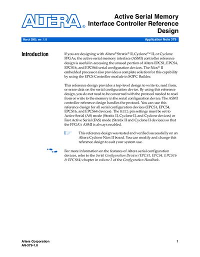
The document provides a reference design for the Active Serial Memory Interface (ASMI) controller, enabling read, write, and erase operations on Altera EPCS serial configuration devices. It includes a top‑level design, port descriptions, block diagrams, timing diagrams, and guidance on integrating the design with Stratix® IL, Cyclone™ IL, Stratix II, and Cyclone II devices.
Additional sections list the delivered source files, explain clock‑divider requirements, detail signal behavior during operations, and give practical notes on resetting the controller, protecting memory sectors, and using Quartus II tools for prototyping and debugging.
| Clock divider maximum frequency | 40 MHz for EPCS1/EPCS4, 80 MHz for EPCS16/EPCS64 |
|---|---|
| Data write bus width | 8 bits |
| Address bus width | 24 bits |
| Number of bytes input width | 9 bits (max 256 bytes) |
| Data read bus width | 8 bits |
The design works with Altera Stratix IL, Cyclone IL, and Cyclone FPGAs, as well as Stratix II and Cyclone II devices for Fast Active Serial mode.
It can divide the system clock up to 40 MHz for EPCS1/EPCS4 devices or 80 MHz for EPCS16/EPCS64 devices.
The address bus is 24 bits wide.