
This application report provides a design reference guide for the TMS320F28xx/28xxx digital signal controller (DSC), including the configuration of the analog-to-digital converter (ADC), the setting of related registers, the response to interrupts, and reference for the circuit board design. This guide is useful for software engineers who are new to the TMS320C2000™ digital signal processor (DSP) and rarely use analog devices.
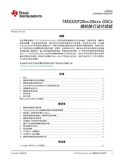
The document provides a design‑reference guide for using the analog‑to‑digital converter (ADC) on Texas Instruments TMS320F28xx/28xxx digital signal controllers. It explains ADC structure, register settings, sampling options, and hardware considerations such as input circuitry and reference voltage.
Key sections include ADC module description, preparation and operation steps, clock and sampling configuration, hardware layout guidelines, and an appendix comparing device families. Sample code for the F280xx development board is also supplied. This manual is written in Chinese.
| Number of ADC channels | 16 |
|---|---|
| ADC resolution | 12‑bit |
| Maximum sampling speed | 12.5 MSPS (up to 6.25 MSPS or 3.75 MSPS for lower modes) |
| Input voltage range | 0 V to 3.0 V |
The ADC can sample up to 12.5 MSPS, with lower modes of 6.25 MSPS or 3.75 MSPS available.
The ADC has 16 result registers, named ADCRESULT0 through ADCRESULT15.
The allowed analog input voltage range is 0 V to 3.0 V.