
The SN74LVC2G08 is a dual 2-input positive-AND gate designed for 1.65-V to 5.5-V VCC operation. The SN74LVC2G08 performs the Boolean function Y = A • B or Y = A & B in positive logic. NanoStar and NanoFree package technology is a major breakthrough in IC packaging concepts, using the die as the package.
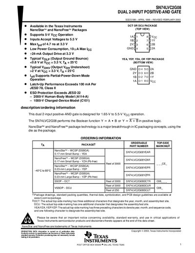
The SN74LVC2G08 is a dual 2‑input positive‑AND gate designed for low‑power logic applications. It operates from 1.65 V to 5.5 V and offers features such as partial‑power‑down mode, low output drive, and robust ESD protection.
The document includes ordering information, recommended operating conditions, electrical and switching characteristics, mechanical drawings for the NanoStar, NanoFree, DCT, and DCU packages, and an important notice about product availability and warranty.
| Output drive current (3.3 V) | 24 mA |
|---|---|
| Maximum propagation delay (3.3 V) | 4.7 ns |
The maximum propagation delay is 4.7 ns at 3.3 V.
The device is designed for operation from 1.65 V to 5.5 V.