
The SN74LVC2G02 is a dual 2-input positive-NOR gate designed for 1.65-V to 5.5-V VCC operation. It supports partial-power-down mode operation, and has low power consumption (10-µA maximum ICC), high output drive capability (±24-mA), low output voltage swing (typical VOLP less than 0.8 V), and high electrostatic discharge (ESD) protection (exceeds JESD 22).
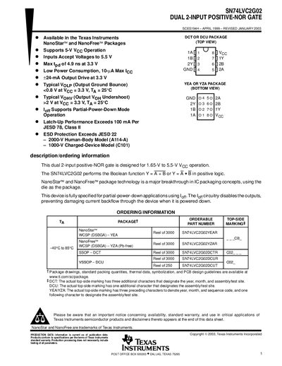
The SN74LVC2G02 is a dual 2‑input positive‑NOR gate designed for operation from 1.65 V to 5.5 V. It offers low power consumption, up to ±24 mA output drive at 3.3 V, and features partial‑power‑down mode with latch‑up protection.
The device is offered in NanoStar, NanoFree, DCT, DCU, SSOP, and VSSOP packages, with detailed mechanical drawings and thermal data provided. Electrical, switching, and mechanical specifications are listed, along with recommended operating conditions and ESD protection ratings.
| Supply voltage range | 1.65 V to 5.5 V |
|---|---|
| Maximum output drive current | ±24 mA at 3.3 V |
| Propagation delay (typ.) | 4.9 ns at 3.3 V |
| ESD protection (Human‑Body Model) | 2000 V |
The device operates from 1.65 V up to 5.5 V.
It can source or sink up to ±24 mA at a 3.3 V supply.
The device exceeds 2000 V HBM and 1000 V CDM ESD protection.
It is offered in NanoStar, NanoFree, DCT, DCU, SSOP, and VSSOP packages.