
This document describes the features and characteristics of the SN74LVC2G125 dual bus buffer gate. The product supports 5V VCC operation and accepts input voltages up to 5.5V. It features 3-state outputs and low power consumption, with a maximum static current of 10µA. The maximum propagation delay is 4.3ns at 3.3V. It supports partial-power-down mode operation and has latch-up performance exceeding 100mA and ESD protection up to 2000V.
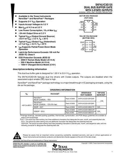
The SN74LVC2G125 is a dual bus buffer gate with 3‑state outputs. It operates from 1.65 V to 5.5 V (0.5 V to 6.5 V absolute maximum) and provides up to +24 mA output drive at 3.3 V while consuming only about 10 µA.
The device is offered in NanoStar, NanoFree, DCT, DCU, YEA, YZA, SSOP and VSSOP packages, with mechanical drawings and thermal data available on the TI website. The datasheet also includes absolute‑maximum ratings, recommended operating conditions, and TI’s standard warranty notice.
| Output drive current at 3.3 V | +24 mA |
|---|---|
| Low‑power consumption | 10 µA max |
| Propagation delay (typical) | 4.3 ns at 3.3 V |
| ESD protection (Human‑Body Model) | 2000 V |
It can source or sink up to +24 mA when operated at 3.3 V.
The SN74LVC2G125 is available in NanoStar, NanoFree, DCT, DCU, YEA, YZA, SSOP and VSSOP packages.
The outputs are disabled, placing the device in a high‑impedance state.