
This document describes the features and characteristics of the SN74LVC1G79 single positive-edge-triggered D-type flip-flop. The flip-flop supports 5V VCC operation and accepts input voltages up to 5.5V. Clock triggering occurs at a voltage level and is not directly related to the rise time of the clock pulse. The product features low power consumption, high output drive current, and excellent immunity to interference.
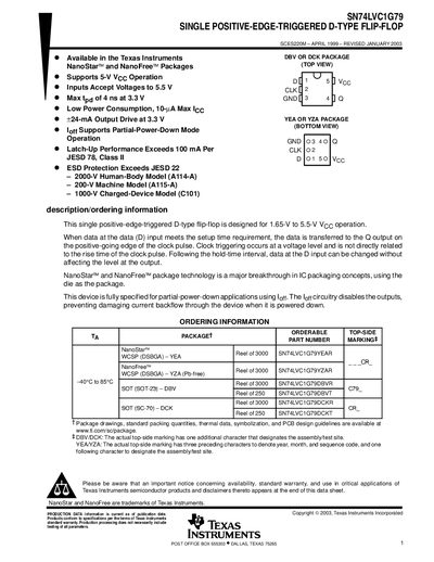
The SN74LVC1G79 is a single positive‑edge‑triggered D‑type flip‑flop designed for 1.65‑V to 5.5‑V operation. Data present at the D input is transferred to the Q output on the rising edge of the clock, with defined setup and hold times.
The device is offered in NanoStar™ and NanoFree™ wafer‑scale packages as well as DBV, DCK, SOT‑23, and SC‑70 footprints. Electrical ratings include low‑power consumption, 24‑mA output drive at 3.3 V, and robust ESD protection. Detailed mechanical drawings, thermal impedance values, and recommended operating conditions are provided, and additional package data can be found on the TI website.
| Supply voltage range | 1.65 V to 5.5 V |
|---|---|
| Output drive current | ±24 mA at 3.3 V |
| Maximum clock frequency | 160 MHz |
It operates from 1.65 V up to 5.5 V.
The device can be clocked up to 160 MHz.
It is offered in NanoStar™, NanoFree™, DBV, DCK, SOT‑23, and SC‑70 packages.