
SN74LVC1G125 is a single bus buffer gate with a 3-state output. It supports 5V VCC operation and accepts input voltages from 1.65V to 5.5V. This device features low power consumption, high output drive capability, and static protection.
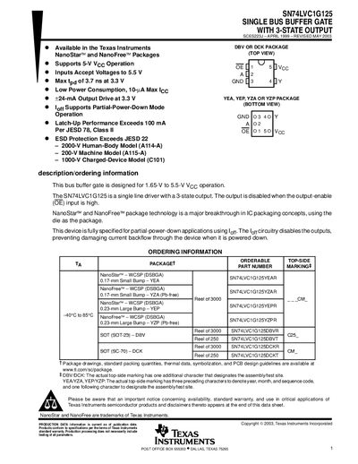
The SN74LVC1G125 is a single‑line driver with a 3‑state output, designed for 1.65 V to 5.5 V VCC operation. The output is disabled when the OE input is high, and the device supports partial‑power‑down mode to prevent back‑flow current.
The datasheet provides electrical characteristics, recommended operating conditions, mechanical drawings for DBV, DCK, NanoStar and NanoFree packages, and ordering information. It also includes a notice about product availability, warranty, and legal terms.
| Maximum output drive current | ±24 mA |
|---|
OE should be tied to VCC through a pull‑up resistor; the minimum value is determined by the driver’s current‑sinking capability.
The maximum propagation delay (tpg) is 3.7 ns at 3.3 V.
The device is available in DBV, DCK, NanoStar (WCSP) and NanoFree (WCSP) packages.