
Key facts
- Model
- ASM5P23S04A
- Category
- Other Electronics
- Documents
- 2
- Languages
- EN
- Last added
- 2012-06-06
Start here
Alliance Semiconductor ASMP5P23S04A handbook
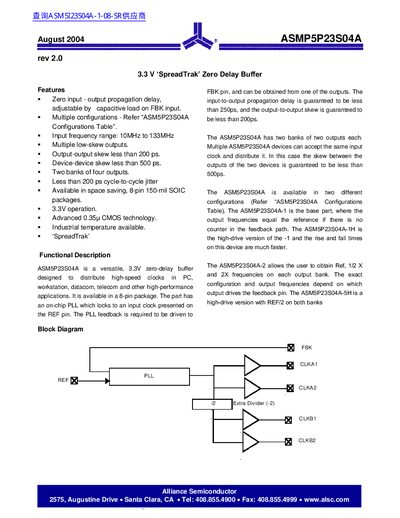
The ASM5P23S04A is a versatile, 3.3V zero-delay buffer designed to distribute high-speed clocks in PC, workstation, datacom, telecom and other high-performance applications. It features an on-chip PLL that locks to an input clock presented on the REF pin, with feedback driven to the FBK pin.
The device is available in multiple configurations including base parts (-1), high-drive versions (-1H, -5H), and frequency divider variants (-2). It offers two banks of outputs with guaranteed output-to-output skew less than 200 ps and device-to-device skew less than 500 ps when all outputs are equally loaded.
Alliance Semiconductor ASM5P23S04A specifications
| Supply Voltage | 3.0 V to 3.6 V |
|---|---|
| Operating Temperature (Commercial) | 0 °C to 70 °C |
| Input Frequency Range | 10 MHz to 133 MHz |
| Output-to-Output Skew | Less than 200 ps |
| Device-to-Device Skew | Less than 500 ps |
| Package Type | 8-pin SOIC |
All Alliance Semiconductor ASM5P23S04A documents by type
Ratings, dimensions and ordering codes, for selection and design work.
Questions answered in these manuals
What is the maximum output frequency for -1H and -5H devices?
The maximum output frequency is 133.3 MHz when using a 20-pF load.
How is the input-output propagation delay adjusted?
The delay is adjustable by varying the capacitive load on the FBK input relative to the other outputs.
What is the input‑to‑output propagation delay of the ASM5P23S04A?
The input‑to‑output propagation delay is guaranteed to be less than 250 ps.
How many outputs does the ASM5P23S04A provide?
It has two banks of two outputs each, for a total of four outputs.