
Key facts
- Model
- AS7C4096A
- Industry
- Industrial
- Documents
- 2
- Languages
- EN
- Last added
- 2012-06-06
Start here
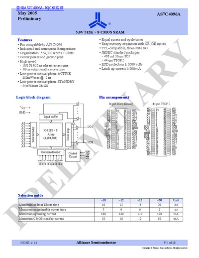
Alliance Semiconductor AS7C4096A SRAM Datasheet
The document describes the AS7C4096A, a high-performance Static Random Access Memory (SRAM) device organized as 524,288 words by 8 bits. It is designed for applications requiring fast data access and low power consumption.
The chip offers equal address access and cycle times ranging from 10 to 20 nanoseconds, with output enable access times of 5 or 6 nanoseconds. The device features TTL-compatible three-state I/O and is available in 400 mil 36-pin SOJ and 44-pin TSOP 2 packages.
Alliance Semiconductor AS7C4096A specifications
| Organization | 524,288 words x 8 bits |
|---|---|
| Supply Voltage | 5.0V |
| Max Address Access Time | 10/12/15/20 ns |
| Max Output Enable Access Time | 5/6 ns |
All Alliance Semiconductor AS7C4096A documents by type
Ratings, dimensions and ordering codes, for selection and design work.
Questions answered in these manuals
What are the available packages for this SRAM?
The device is available as a 400-mil 36-pin SOJ and a 44-pin TSOP 2.
Is the device TTL-compatible?
Yes, all chip inputs and outputs are TTL-compatible.
What are the address and output‑enable access times?
Address access time is 10 ns, 12 ns, 15 ns or 20 ns depending on the speed grade, and output‑enable access time is 5 ns or 6 ns.
Which package options are available for the AS7C4096A?
It is offered in a 36‑pin SOJ (400 mil) package and a 44‑pin TSOP‑2 package.