
The Alpha & Omega Semiconductor AO4401 is a P‑Channel enhancement mode field‑effect transistor with -30 V VDS, -6.1 A ID, and low RDS(on) values.
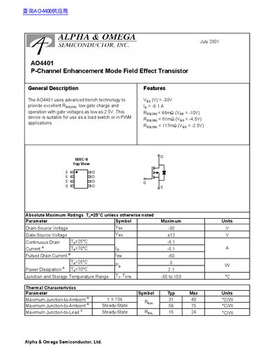
The AO4401 P‑Channel enhancement mode FET is designed for use as a load switch or in PWM applications. It features advanced trench technology that provides low gate charge and operation with gate voltages as low as 2.5 V.
The device is supplied in an SO‑8 package and offers a maximum drain‑source voltage of -30 V, a continuous drain current of -6.1 A, and typical on‑resistance values below 46 mΩ at VGS = -10 V. Thermal resistance from junction to ambient is 40 °C/W, and key capacitances include Ciss = 940 pF and Coss = 104 pF.
| Maximum Drain‑Source Voltage (VDS) | -30 V |
|---|---|
| Gate Threshold Voltage (VGS(th)) | -0.7 to -1.3 V |
| Input Capacitance (Ciss) | 940 pF |
| Package Type | SO‑8 |
| Thermal Resistance Junction‑to‑Ambient (RθJA) | 40 °C/W |
The AO4401 can withstand a maximum drain‑source voltage of -30 V.
The AO4401 is supplied in an SO‑8 (SOIC‑8) surface‑mount package.