
Fairchild Semiconductor FDB3652/FDP3652/FDI3652 N-Channel PowerTrench MOSFET Datasheet

This document is about the FDB3652/FDP3652/FDI3652 N-Channel PowerTrench® MOSFET product information manual released by Fairchild Semiconductor Corporation in 2002
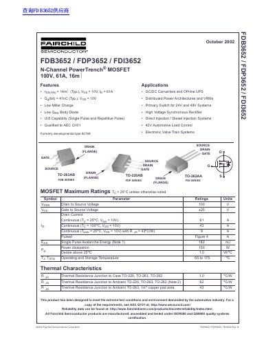

Fairchild Semiconductor FDB3652/FDP3652/FDI3652 N-Channel PowerTrench MOSFET Datasheet - cover page
Brand
Fairchild
Category
MOSFET
Document type
Datasheet
Language
English
Pages
11
File format
PDF
File size
211 KB
Published
07 August, 2012
Updated
30 September, 2023
MD5 checksum
E849D50F53CC0044CCAF06614A050F23

About this manual

This document is a datasheet for the Fairchild Semiconductor FDB3652, FDP3652, and FDI3652 series of N-Channel PowerTrench MOSFETs. These devices are rated at 100V drain-to-source voltage and 61A continuous current with a typical on-resistance of 14mΩ.

What's inside

  • Features
  • Applications
  • Maximum Ratings
  • Electrical Characteristics
  • Dynamic Characteristics
  • Switching Characteristics
  • Drain-Source Diode Characteristics
  • Typical Characteristics
  • Test Circuits and Waveforms
  • Thermal Resistance

Specifications

Drain to Source Voltage (Vdss)100 V
Continuous Drain Current (Tj=25°C, Vgs=10V)61 A
On-Resistance (Typical)14 mΩ
Total Gate Charge (Typical)41 nC
Power Dissipation150 W
Operating Temperature Range-55 to +175 °C

Frequently asked questions

What is the maximum power dissipation rating for this MOSFET?

The maximum rated power dissipation is 150 W.

Download PDF (211 KB)

More Fairchild Manuals


View all Fairchild manuals →