
This document describes the bank number VREF pin names and functions for different models, as well as configuration functions and channel information.
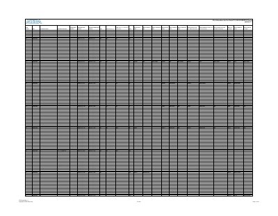
This document provides pin information for the Stratix IV GX EP4SGX180 device. It includes a pictorial representation of the device package showing the placement of various signal banks and reference voltages.
This document provides pin information for the Stratix IV GX EP4SGX180 Device.
The current version of this document is Version 1.1.
Version 1.1 added bank numbers for JTAG pins, updated Note (1) in the Pin List, and grouped nCSO, ASDO, and DCLK into dedicated configuration/JTAG pins.