
Altera EPM240/EPM240G MAX II Pin Information Datasheet

This document is about the pin information of EPM240 device, including IO/GCLK0, IO/GCLK1, IO/GCLK2, IO/GCLK3, IO/DEV_OE, IO/DEV_CLRn, TDI, TMS, TCK, TDO, GNDINT, GNDIO, VCCINT, VCCIO1, VCCIO2
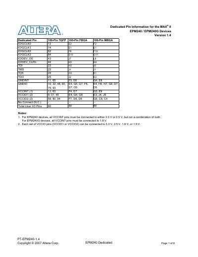

Altera EPM240/EPM240G MAX II Pin Information Datasheet - cover page
Brand
Altera
Category
Other Electronics
Document type
Datasheet
Language
English
Pages
8
File format
PDF
File size
452 KB
Published
01 August, 2012
Updated
30 September, 2023
MD5 checksum
C95CDADD9DFD643B7D27723C16CD7444

About this manual

This document provides dedicated pin information for the MAX II EPM240 and EPM240G devices, covering 100-pin TQFP, FBGA, and MBGA packages. It details the pinout for each package type, including specific assignments for power, ground, and I/O pins.

What's inside

  • Dedicated Pin Information
  • Pin Definitions
  • Package Diagram and Bank Information
  • Revision History
  • Supply and Reference Pins
  • Programming and JTAG Pins
  • Clock Pins

Specifications

Total User I/O Pins80
VCCINT Voltage (EPM240)3.3 V or 2.5 V
VCCINT Voltage (EPM240G)1.8 V
Document Version1.4

Frequently asked questions

What voltage must EPM240G VCCINT pins be connected to?

All VCCINT pins must be connected to 1.8 V.

Can VCCIO pins be powered by different voltages?

Yes, each set of VCCIO pins can be connected to 3.3 V, 2.5 V, 1.8 V, or 1.5 V.

What are the supported package types for these devices?

The supported packages are 100-Pin TQFP, 100-Pin FBGA, and 100-Pin MBGA.

Download PDF (452 KB)

More Altera Manuals


View all Altera manuals →