
Pin-Outs for EPF10K50S device, including 144-Pin TQFP, 208-Pin PQFP, 240-Pin PQFP, 256-Pin FineLine BGA, 356-Pin BGA and 484-Pin FineLine BGA
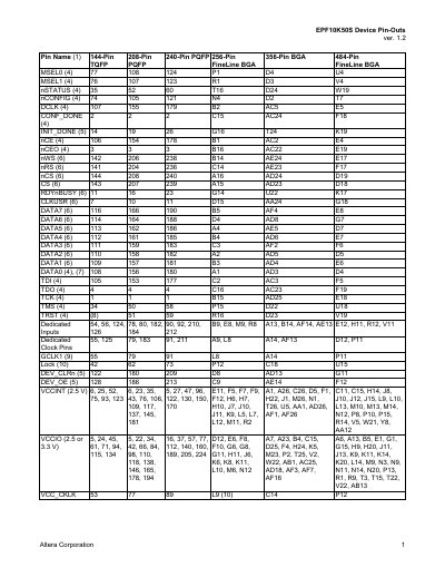
This document serves as a reference guide for the EPF10K50S FPGA, detailing the pin assignments for 144-pin TQFP, 208-pin PQFP, 240-pin PQFP, 256-pin TQFP, 356-pin BGA, and 484-pin BGA packages. It lists specific pin names, their corresponding package locations, and distinguishes between dedicated pins and user I/O pins.
| Model | EPF10K50S |
|---|---|
| Available Packages | 144-Pin TQFP, 208-Pin PQFP, 240-Pin PQFP, 256-Pin TQFP, 356-Pin BGA, 484-Pin BGA |
| Total User I/O (144-Pin) | 102 |
No, pins not listed in the table are user I/O pins, while listed pins have specific device functions.
No, the optional JTAG pin TRST is not used in the 144-pin TQFP package.
The VCCINT pin requires 2.5 V.