
This is a pinout for EP1K30 device. It lists all the pin functions and corresponding pin numbers.
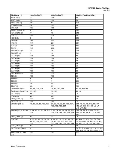
The document serves as a reference guide for the pin assignments of the Altera EP1K30 Field-Programmable Gate Array (FPGA). It details the physical layout of pins across three different package types: 144-pin TQFP, 208-pin PQFP, and 256-pin FineLine BGA.
The text categorizes each pin by function, including dedicated inputs, dedicated clock pins, configuration control signals (such as nCONFIG and CONF_DONE), JTAG interface pins, and power/ground connections for internal logic and I/O banks. It also specifies the total count of user I/O pins available in each package variant.
| Total User I/O Pins (144-pin TQFP) | 102 |
|---|---|
| Total User I/O Pins (208-pin PQFP) | 147 |
| Total User I/O Pins (256-pin FineLine BGA) | 171 |
The device is available in three packages: 144-pin TQFP, 208-pin PQFP, and 256-pin FineLine BGA.
No, the optional JTAG pin TRST is not used in the 144-pin TQFP package.
The document states that all pins not listed in the table are considered user I/O pins.