
EP1K10 device pin-out
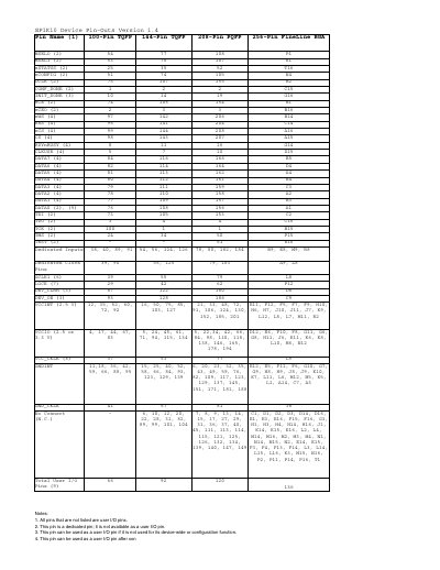
The document serves as a reference guide for the physical pin assignments of the EP1K10 Field-Programmable Gate Array (FPGA). It details the layout for four specific package configurations: 100-Pin TQFP, 144-Pin TQFP, 208-Pin PQFP, and 256-Pin FineLine BGA.
The text lists dedicated pins required for configuration and operation, such as MSEL, INIT_DONE, CE, ICBO, and various data lines (DATAT through DATA7). It also identifies specific power supply pins like VCCINT and hWOCIO, along with notes on their voltage requirements. The document clarifies which pins are available for user I/O versus those dedicated to internal functions.
| Package Types Supported | 100-Pin TQFP, 144-Pin TQFP, 208-Pin PQFP, 256-Pin FineLine BGA |
|---|---|
| Total User I/O Pins (144-Pin) | 52 |
The device is available in 100-Pin TQFP, 144-Pin TQFP, 208-Pin PQFP, and 256-Pin FineLine BGA packages.
The pin should be connected to VCCINT or GNDINT.
The LOCK pin goes low if a periodic clock stops clocking.