
The characteristics of IPB08CN10N G IPI08CN10N G IPP08CN10N G OptiMOS®2 power transistor include N-channel, normal level, excellent gate charge x R DS(on) product (FOM), very low on-resistance R DS(on), 175 °C operating temperature, lead-free lead plating; RoHS compliant, qualified according to JEDEC1) for target application, ideal for high-frequency switching and synchronous rectification.
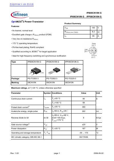
This document is a datasheet for the Infineon OptiMOS power transistors, specifically the IPB08CN10N G, IPI08CN10N G, and IPP08CN10N G models. These N-channel devices are designed for high-frequency switching and synchronous rectification applications, offering very low on-resistance and excellent gate charge characteristics. The transistors are available in PG-TO263-3, PG-TO262-3, and PG-TO220-3 packages and are RoHS compliant with Pb-free lead plating.
| Continuous drain current | 95 A |
|---|---|
| Operating temperature | -55 ...175 °C |
| Drain-source breakdown voltage | 100 V |
| Drain-source on-state resistance | 8.2 mΩ |
| Power dissipation | 167 W |
| Package types | PG-TO263-3, PG-TO262-3, PG-TO220-3 |
The maximum continuous drain current is 95 A when the temperature is 25 °C.
The device can operate at a maximum junction temperature of 175 °C.
The maximum gate-source voltage is +20 V.