
CY23S08 is a 3.3V zero delay buffer designed by Cypress Semiconductor Corporation to distribute high speed clocks in PC, workstation, datacom, telecom, and other high performance applications. Its main features are zero input-output propagation delay, adjustable FBK input capacitive load, multiple configuration methods, low-skew outputs, 10 MHz to 133 MHz operating range, 65 ps typical cycle-cycle jitter and advanced 0.65μ CMOS technology.
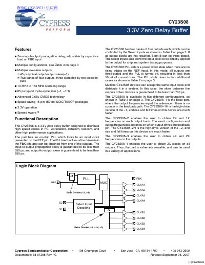
The CY23S08 is a 3.3V zero delay buffer featuring an on-chip Phase Locked Loop (PLL) that locks to an input clock presented on the REF pin. It includes two banks of four outputs each, which can be controlled by select inputs and three-stated independently. The device supports multiple configurations for frequency multiplication and distribution.
| Supply Voltage | 3.0V to 3.6V |
|---|---|
| Operating Temperature Range | 0°C to 70°C |
| Output Frequency Range | 10 MHz to 133 MHz |
| Typical Output-Output Skew | 45 ps |
| Typical Cycle-to-Cycle Jitter | 65 ps |
| Package Type | 16-pin 150-mil SOIC/TSSOP |
The maximum supply voltage to ground is +7.0V DC.
The device has two banks of four outputs each.
In power down mode, the current draw is less than 50μA.