
The document mainly introduces the characteristics of CY7C1379B, including supporting up to 133MHz bus operations, zero wait states, compatibility with ZBT™ devices, internally self-timed output buffer control, registered inputs, byte write capability, 256K x 32 common I/O architecture, single 3.3V power supply, fast clock-to-output time, clock enable (CEN) pin, synchronous self-timed write, asynchronous output enable, JEDEC standard 100 TQFP and 165 fBGA packages, burst capability, linear or interleaved burst order, and low standby power.
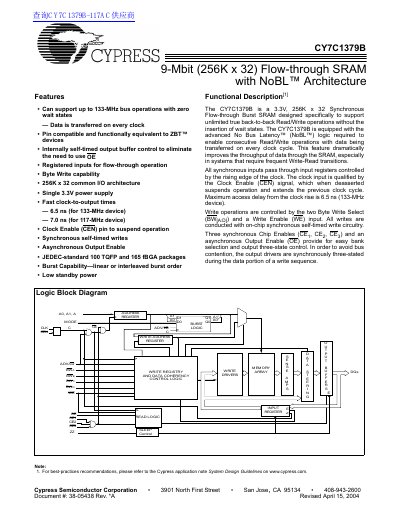
The CY7C1379B is a 3.3V, 256K x 32 Synchronous Flow-through Burst SRAM designed specifically to support unlimited true back-to-back Read/Write operations without the insertion of wait states. It utilizes advanced No Bus Latency (NoBL) logic to enable consecutive Read/Write operations with data being transferred on every clock cycle.
| Capacity | 9-Mbit (256K x 32) |
|---|---|
| Voltage | 3.3V |
| Maximum Bus Frequency | 133 MHz |
| Maximum Access Time (133 MHz) | 6.5 ns |
| Maximum Operating Current (133 MHz) | 250 mA |
It supports both linear and interleaved burst order.
All writes are conducted with on-chip synchronous self-timed write circuitry.