
This data sheet provides a detailed overview of the Cypress CY7B993V and CY7B994V high-performance multi-phase PLL clock buffers.
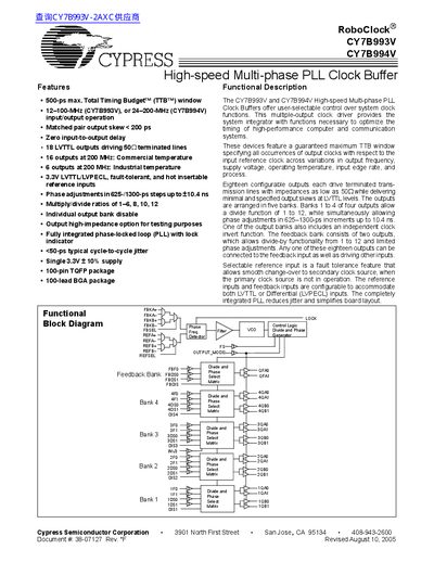
The Cypress CY7B993V and CY7B994V are High-speed Multi-phase PLL Clock Buffers that offer user-selectable control over system clock input/output operations. These devices feature a guaranteed maximum Total Timing Budget (TTB) window, specifying all occurrences of output clocks with respect to the input reference clock across variations in output frequency, supply voltage, operating temperature, input edge rate, and process.
| Max Total Timing Budget (TTB) window | 500-ps |
|---|---|
| Output skew | < 200 ps |
| Supply voltage | 3.3V |
| Operating temperature ranges | Commercial, Industrial |
The CY7B993V and CY7B994V offer a guaranteed maximum Total Timing Budget (TTB) window of 500 ps.
The CY7B994V High-speed Multi-phase PLL Clock Buffer operates at frequencies from 24 MHz to 200 MHz.
The device features sixteen outputs capable of driving terminated lines at a frequency of 200 MHz.