
This datasheet provides information on the features of 18-Mbit (512K x 36/1M x 18) Flow-Through SRAM CY7C1381D, CY7C1381F CY7C1383D, CY7C1383F, including support for 133 MHz bus operations, 512K × 36 and 1M × 18 common IO, 3.3V core power supply (VDD), 2.5V or 3.3V IO supply (VDDQ), Fast clock-to-output time — 6.5 ns (133 MHz version), Provides high performance 2-1-1-1 access rate, etc.
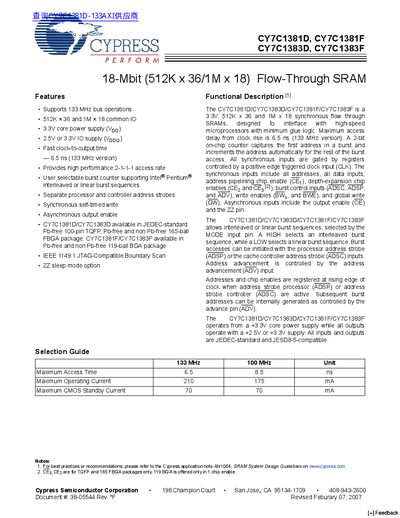
This document describes the CY7C1381D, CY7C1381F, CY7C1383D, and CY7C1383F synchronous flow-through SRAMs. These devices are designed to interface with high-speed microprocessors with minimum glue logic.
| Maximum Access Time (133 MHz) | 6.5 ns |
|---|---|
| Maximum Operating Current (133 MHz) | 210 mA |
| Core Power Supply Voltage | 3.3V |
The maximum access time is 6.5 ns for the 133 MHz version and 8.5 ns for the 100 MHz version.
The device requires a +3.3V core power supply and operates with either a +2.5V or +3.3V I/O supply.
A HIGH level on the MODE pin selects an interleaved burst sequence, while a LOW level selects a linear burst sequence.