
TB62733FTG is a dual output boost converter launched by Toshiba. The input voltage range is 2.8V to 4.2V, the output voltage range is 4.0V to 5.5V, the maximum output current is 190mA, and it integrates over temperature protection function.
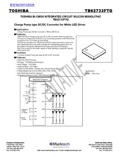
The Toshiba TB62733FTG is a Bi-CMOS integrated circuit designed as a charge pump type DC to DC converter specifically for driving white LEDs. It accepts an input voltage ranging from 2.8V up to 4.2V and performs a 1.5 times step-up conversion, providing a maximum output current of over 190mA. The device features two separate outputs (Vout1 and Vout2) which can be independently controlled via logic inputs CE1 and CE2.
| Input Voltage Range | 2.8V to 5.5V |
|---|---|
| Output Current (Max) | >190mA |
| Conversion Ratio | 1.5 times step up |
| Operating Temperature Range | -25°C to 85°C |
| Package Type | VQON24 (Leadless type) |
The device provides over 190mA at Vin=3.9V as the maximum current.
Yes, it has an integrated Thermal Shut Down (TSD) function to protect from thermal damage.
The device supports 4 steps of brightness control: 25%, 50%, 75%, and 100%.