
This datasheet describes the features and characteristics of Fujitsu Semiconductor's Stacked MCP (Multi-Chip Package) FLASH MEMORY & SRAM CMOS 16M ( × 8/ × 16) FLASH MEMORY & 4M ( × 8/ × 16) STATIC RAM.
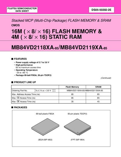
The Fujitsu MB84VD2118XA-85 and MB84VD2119XA-85 are stacked multi‑chip package (MCP) flash memory and SRAM devices. They operate from 2.7 V to 3.6 V, provide up to 16 Mbit flash and 4 Mbit static RAM, and feature an 85 ns maximum access time.
The devices are offered in 69‑ball FBGA and 56‑pin plastic TSOP packages, support simultaneous read/write operations, sector erase architecture, and include power‑saving modes such as automatic sleep. Detailed pin assignments, bus operations, and electrical characteristics are provided for system integration.
| Power supply voltage | 2.7 V to 3.6 V |
|---|---|
| Maximum access time | 85 ns |
| Operating temperature | -25 °C to +85 °C |
| Package types | 69‑ball FBGA, 56‑pin TSOP |
| Flash memory size | 16 Mbit (x8/x16) |
| SRAM size | 4 Mbit (x8/x16) |
| Max CE access time | 85 ns |
| Max OE access time | 35 ns (MB84VD2118XA) / 45 ns (MB84VD2119XA) |
| Operating current | 40 mA max |
| Standby current | 7 µA max |
| Data retention voltage | 1.5 V to 3.6 V |
The devices operate from –25 °C to +85 °C.
The maximum access time is 85 ns.
The parts require a power supply voltage between 2.7 V and 3.6 V.
They are offered in a 69‑ball FBGA package and a 56‑pin plastic TSOP package.