
M58WR064ET M58WR064EB 64 Mbit (4Mb x 16, Multiple Bank, Burst) 1.8V Supply Flash Memory FEATURES SUMMARY
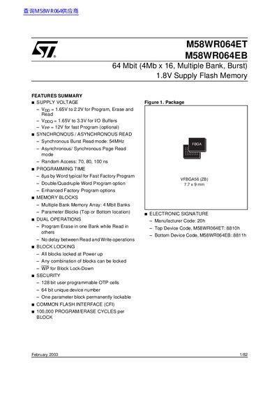
This datasheet describes the 64 Mbit (4 Mbit × 16) non‑volatile flash memory devices M58WRO64ET and M58WRO64EB. It covers electrical characteristics, memory architecture, command set, timing diagrams, and security features. The devices operate with a 1.65 V‑2.2 V Vpp supply for normal programming and an optional 12 V Vpp for fast programming.
The document includes detailed tables for signal definitions, bus operations, command codes, configuration registers, and block locking schemes. Appendices provide the Common Flash Interface (CFI) query structure, flowcharts for programming/erase operations, and revision history. The information is intended for designers integrating the flash memory into electronic systems.
| Supply Voltage (Vpp) for Program/Erase/Read | 1.65 V to 2.2 V |
|---|---|
| I/O Buffer Supply Voltage (Vppa) | 1.65 V to 3.3 V |
| Fast Program Supply Voltage (optional) | 12 V |
| Synchronous Burst Read Frequency | up to 54 MHz |
| Random Access Timing | 70 ns – 100 ns |
| Typical Word Program Time (Fast Factory) | 8 µs |
| Number of Memory Banks | 4 banks of 4 Mbit each |
| Endurance per Block | 100,000 program/erase cycles |
| Security Features | 128‑bit OTP cells, 64‑bit unique device number |
Each memory block is rated for up to 100,000 program/erase cycles.
The synchronous burst read mode operates up to 54 MHz.
The flash memory is organized into four 4‑Mbit banks.